FPGA bitstream
How to build the Domesday Duplicator's gateware and get it onto the DE0-NANO, with a check to confirm each step actually worked.
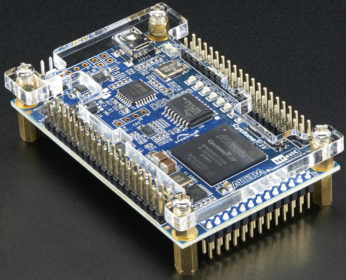
The gateware runs on a Terasic DE0-NANO carrying an Intel (Altera) Cyclone IV EP4CE22F17C6. It generates the ADC sampling clock, buffers samples across the clock-domain boundary, and feeds them to the FX3 over the GPIF II bus.
The board has an onboard USB-Blaster, so no separate programming pod is needed — the DE0-NANO's mini-USB connector is both its power supply and its programming interface.
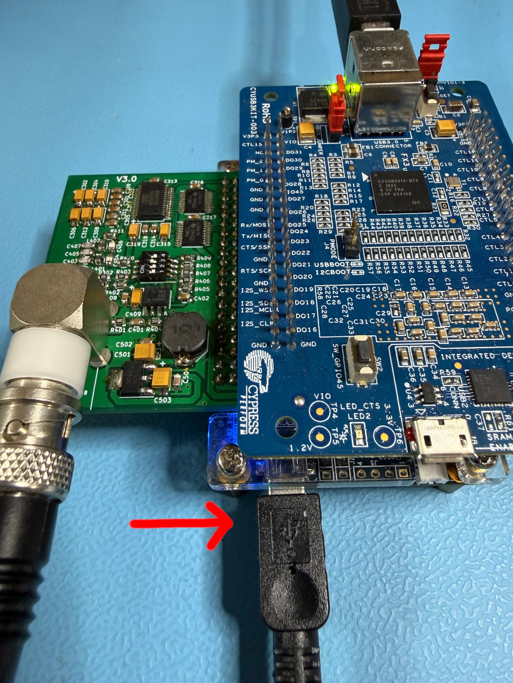
In an assembled Duplicator, it is not the only power supply
That description is of the board on its own. Bolted to a Duplicator PCB with the FX3 kit above it, the assembly is powered through either USB connector, and either one alone keeps the whole thing alive.
Two consequences, and the second is a trap. The board is lit whatever the mini-USB is doing, so "the lights are on" says nothing at all about whether the USB-Blaster is connected — a charge-only cable looks identical to a working one. And a power cycle means unplugging both cables: pull only one and nothing reboots, while the board stays lit and looks perfectly normal.
The application can do this for you
Writing the EPCS no longer needs Quartus: ddd-gui plays a CI-built SVF through the same
onboard USB-Blaster — Tools ▸ Firmware ▸ Bring up a new or legacy board….
See Bringing up a new or legacy board, and
USB-Blaster and SVF programming for how it works.
This page remains the reference for building the bitstream and for programming it by hand.
There are two ways to program it, and you will usually want both:
| Writes to | Survives a power cycle | Use for | |
|---|---|---|---|
FPGA configuration SRAM (.sof) |
Volatile memory in the FPGA | No | Testing a bitstream before committing to it |
EPCS64 serial configuration device (.jic) |
The DE0-NANO's onboard flash | Yes | Normal use |
Start with the .sof. It cannot leave the board in a bad state — a power cycle restores
whatever the flash holds — so it is the safe way to find out whether a bitstream works before
making it permanent. This mirrors the RAM-then-EEPROM order on the
FX3 firmware page, and for the same reason.
Before you start
- Set up device access — Linux device access. Without it,
Quartus reports
Unable to lock chain - Insufficient port permissionsand cannot program anything. - Get Quartus Prime Lite. It is free and needs no licence file, but it is a
multi-gigabyte download and is
x86_64Linux or Windows only. The project builds against version 25.1.
You may not need to build anything
Prebuilt .sof and .jic files are attached to
releases, along with a
bitstream-provenance.txt recording the commit and Quartus version they came from. If you
only want to program a board, skip to step 2.
1. Build the bitstream
With Nix
From anywhere in a checkout, on x86_64-linux:
The gateware is two images that live in one flash: the capture gateware in
application/, and a small resident boot loader in factory/ that a unit falls back to if
a gateware update is ever interrupted. provisioning/ holds the one .jic that carries
both, and that is the file a board is programmed with. The model is described on the
EPCS layout and boot flow page.
There is deliberately no .jic of the capture gateware alone: programming one would
write it over the factory image, leaving a unit with nothing to fall back to.
Quartus comes from the flake, so nothing needs installing first. The first build is slow: Quartus is not redistributable, so it can never come from a binary cache and must be fetched from Altera. The build is restricted to the Cyclone IV device family, which removes five of the six component downloads.
With Quartus installed by hand
Put Quartus' bin directory on PATH, then:
That copies the sources to fpga/build/, compiles both images, converts them into one
provisioning .jic — and into the .svf carrying the same content as JTAG vectors — and
writes the provenance record. Or drive the tools yourself — the GUI
is not required for any step:
cd factory      && quartus_sh --flow compile DomesdayDuplicatorFactory
cd application  && quartus_sh --flow compile DomesdayDuplicator
cd provisioning && quartus_cpf -c DomesdayDuplicatorProvisioning.cof   # both .sof -> one .jic
cd provisioning && quartus_cpf -c -q 4.5MHz -g 3.3 -n p \
    DomesdayDuplicatorProvisioning_write_jic.cdf \
    DomesdayDuplicatorProvisioning.svf                                # the same, as vectors
Do not compile in fpga/application/ or fpga/factory/
quartus_sh rewrites the .qsf project file in place to record the Quartus version
that last touched it, and scatters about thirty build products beside the sources. Both
routes above copy the project to a build directory first. If you compile in the source
directories you will find the repository has uncommitted changes you did not make.
Check: what did you just build?
The build writes a bitstream-provenance.txt recording where the bitstream came from:
Source
------
  commit                    1b86b65a
  device                    EP4CE22F17C6
  family                    Cyclone IV E

Toolchain
---------
  quartus                   Version 25.1std.0 Build 1129 10/21/2025 SC Lite Edition
A -dirty suffix on the commit means the working tree had uncommitted changes, so the hash
alone does not describe what you built. Worth noticing before you program anything.
2. Program the board
Each .cdf file names its own inputs, so run it from the directory holding the bitstream it
names — under result/ for a Nix build, fpga/build/ for a local one.
2a. The .sof — the test path
or, to look at the factory image on its own:
Info (213045): Using programming cable "USB-Blaster [7-3.2]"
Info (213011): Using programming file ./DomesdayDuplicator.sof with checksum 0x001D67A1 for device EP4CE22F17@1
Info (209016): Configuring device index 1
Info (209017): Device 1 contains JTAG ID code 0x020F30DD
Info (209007): Configuration succeeded -- 1 device(s) configured
Info (209011): Successfully performed operation(s)
0x020F30DD is the Cyclone IV EP4CE22's JTAG ID. If you see a different one, the .cdf is
talking to a different board.
This is volatile. Power cycle and it is gone, replaced by whatever is in the EPCS64 flash. That is the point: if the bitstream is broken, you have lost nothing.
2b. The provisioning .jic — the production path
Do this once you are satisfied the bitstream works.
Or without Quartus at all
ddd-jtag DomesdayDuplicatorProvisioning.svf writes the same content through the same
on-board cable, driving it over libusb rather than through Quartus — see
USB-Blaster and SVF programming. The .svf comes from the
same build as the .jic and describes the same flash, so the two routes are
interchangeable; everything on the rest of this page — the power cycle, the silicon
identifier, what the board comes up as — applies to both. Quartus's own jtagd holds
the cable open whenever it is running, so stop it first.
This writes the EPCS64 serial configuration device, which the FPGA loads from at every
power-up, with both images: the factory image at address 0 and the capture gateware at
0x200000. It takes appreciably longer than the .sof path, because it programs the flash
through the FPGA rather than configuring the FPGA directly.
The programmer prints the flash's silicon identifier as it works. It must read 0x16, the
EPCS64's, which is the same value the firmware checks before it will write a byte.
Then power cycle the board, and treat that as part of the procedure rather than as housekeeping. The programmer reaches the flash by loading a serial flash loader into the FPGA, and it leaves that running — so until the board is power cycled the FPGA is running Altera's loader and not this project's gateware at all. It answers nothing on the register link, and an update attempted in that state is refused with "the FPGA is not answering".
What it comes up as depends on what was in the flash before, because the erase is page-selective and the boot block sector is outside the pages this file writes:
- a board being provisioned for the first time has no boot block, so it comes up running the factory image — the resident boot loader rather than the capture gateware. The capture application reports it as running recovery gateware. Writing the boot block is the last step of a gateware update rather than part of this file, so that is the expected state;
- a board being re-provisioned keeps its existing boot block, and if the application image just written still matches the CRC that block records, it boots straight into the capture gateware.
Both are correct. The EPCS layout and boot flow page describes the states and what makes an application image count.
This is the last time a cable is needed. From here the capture gateware is updated over the same USB cable the Duplicator already uses.
Confirming what is running
The LEDs
The gateware generates no pattern of its own. It lights LED 0 alone coming out of reset and then leaves the row to the FX3, which drives it over the register link as a status display. So the LEDs answer a different question than they used to, and a more useful one:
| What you see | What it means |
|---|---|
| Nothing lit | The FPGA is unconfigured — its pins are high-Z |
| One LED, steady | Gateware configured and running, and the FX3 has not spoken to it yet |
| A firmware pattern | The FX3 is talking to it. The patterns are listed on the FPGA register interface page |
| One LED, blinking every few seconds | Not a pattern. The FPGA is configuring repeatedly — see below |
The blinking case is worth knowing on sight, because it is what a broken handover looks like and it is easy to read as a heartbeat. Each brief flash is a configuration completing, the FX3 not getting far enough to write the register, and the board reverting; the lap time is a few seconds. A unit doing this is not running the capture gateware at all, whatever the cable says.
The old bouncing-LED check — one lit LED sweeping up the row and back — belonged to gateware predating the register interface, where it doubled as a PLL-lock indicator. The equivalent check now is the register bank answering at all: the identity block cannot be read unless the design is clocked and the PLL is locked.
The device on USB
The FPGA does not appear on USB itself. What it does is supply the FX3's interface clock, so the check is that the FX3 still enumerates at full speed:
$ lsusb -v -d 1209:2347 | grep -E "bcdUSB|iProduct"
  bcdUSB               3.00
  iProduct                2 Domesday Duplicator (d0566b3e)
This does not prove the capture path works
The FX3 enumerates when it boots, which may have been before you reprogrammed the FPGA. A device still present at SuperSpeed afterwards is consistent with working gateware but is not evidence of it.
The only test that exercises the path carrying samples is a capture. Dropped samples do not announce themselves — a capture with a fault completes normally and produces a file that looks fine and is wrong. See below.
The capture-integrity test — the one that counts
After any gateware change, run a test capture:
- Launch the capture application and enable test mode. This switches the FPGA from ADC data to an internally generated counter ramp.
- Capture for at least 60 seconds, so the buffers wrap many times. A short capture can pass while a longer one drops samples.
- Analyse the capture: Edit → Analyse test data..., or from a shell,
DomesdayDuplicator --analyse-test-data <file>.
Zero sequence breaks is a pass. Any break at all means a sample was lost somewhere between the FPGA and the disk, and is a blocker rather than a flake — the ramp is deterministic, so there is no such thing as an intermittent false positive here.
Reproducibility
Quartus fitting is deterministic: the same source, on the same Quartus version and the same
architecture, produces the same placement and routing. The project pins the two settings that
depends on — the Fitter seed and the parallel-processor count — in the .qsf.
What that means for the files:
| File | Across rebuilds |
|---|---|
DomesdayDuplicator.jic |
Byte-identical |
DomesdayDuplicator.sof |
Differs in about 34 bytes, all header metadata — a compile timestamp, a per-run design hash, and the checksum covering them |
So bitstream-provenance.txt publishes two digests per file: a release digest over the
file as shipped, for checking a download, and a canonical digest over the configuration
content, for checking a rebuild. For the .jic they are the same number.
To verify a released bitstream yourself, rebuild it with the same Quartus version and compare the canonical digests:
Troubleshooting
| Symptom | Cause and fix |
|---|---|
Unable to lock chain - Insufficient port permissions |
Device permissions. See Linux device access |
No JTAG hardware available |
The USB-Blaster is not visible at all. Check the DE0-NANO's mini-USB cable is connected and is a data cable, not charge-only |
jtagconfig reports USB-Blaster variant rather than USB-Blaster |
Also permissions — Quartus cannot open the device far enough to identify the cable |
Can't find the programming file |
The .cdf names its inputs relative to the working directory. Run quartus_pgm from the directory holding the .sof/.jic |
A different JTAG ID than 0x020F30DD |
Not a Cyclone IV EP4CE22 — check which board is plugged in |
| LEDs dark or frozen after programming | The PLL is not locking, or the FPGA is held in reset. Check the FX3 board's reset button, and that both boards are seated in their headers |
| Board captures nothing but garbage | The FX3 firmware and the gateware may be out of step. They share a protocol defined in both — update both across a release that changed it |
Quartus rewrote files in fpga/application/ or fpga/factory/ |
You compiled in a source directory. See the warning in step 1 |
You cannot brick the DE0-NANO by programming it
The .sof path never touches non-volatile memory. The .jic path writes the EPCS64, but the
FPGA can always be reconfigured over JTAG regardless of what the flash contains — the
USB-Blaster talks to the FPGA directly. If a bad image reaches the flash, program a good
.sof over JTAG and rewrite the .jic.
Related
- FX3 firmware — the other half, and it must be kept in step with this one
- Linux device access — the USB-Blaster needs a udev rule, and it is in the same file as the FX3's
- Software guide — what each Verilog module does